
With its LCD technologies as a foundation, Innolux has gone beyond the traditional LCD manufacturing frameworks, and transformed and reengineered to be an OEM of components such as high-resolution CMOS, PMOS, and NMOS. Innolux uses its exclusive technology to achieve CMOS processing on glass substrates. This allows components traditionally manufactured on wafers to be transferred to glass substrates. Since the substrate area of the panel is large and square, the production area utilization rate can reach up to 95%, which is a great advantage in terms of area utilization rate.
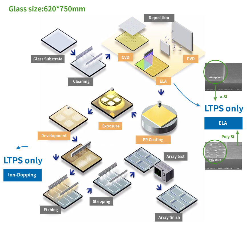
Innolux has a full series of substrate size specifications, including the Generation 3.5 (620×750mm) glass substrate, which is approximately 6.58 times the 12-inch wafer (300mm) and 14.58 times the 8-inch wafer (200mm), giving large-area glass substrates great production efficiency and competitive advantages.