

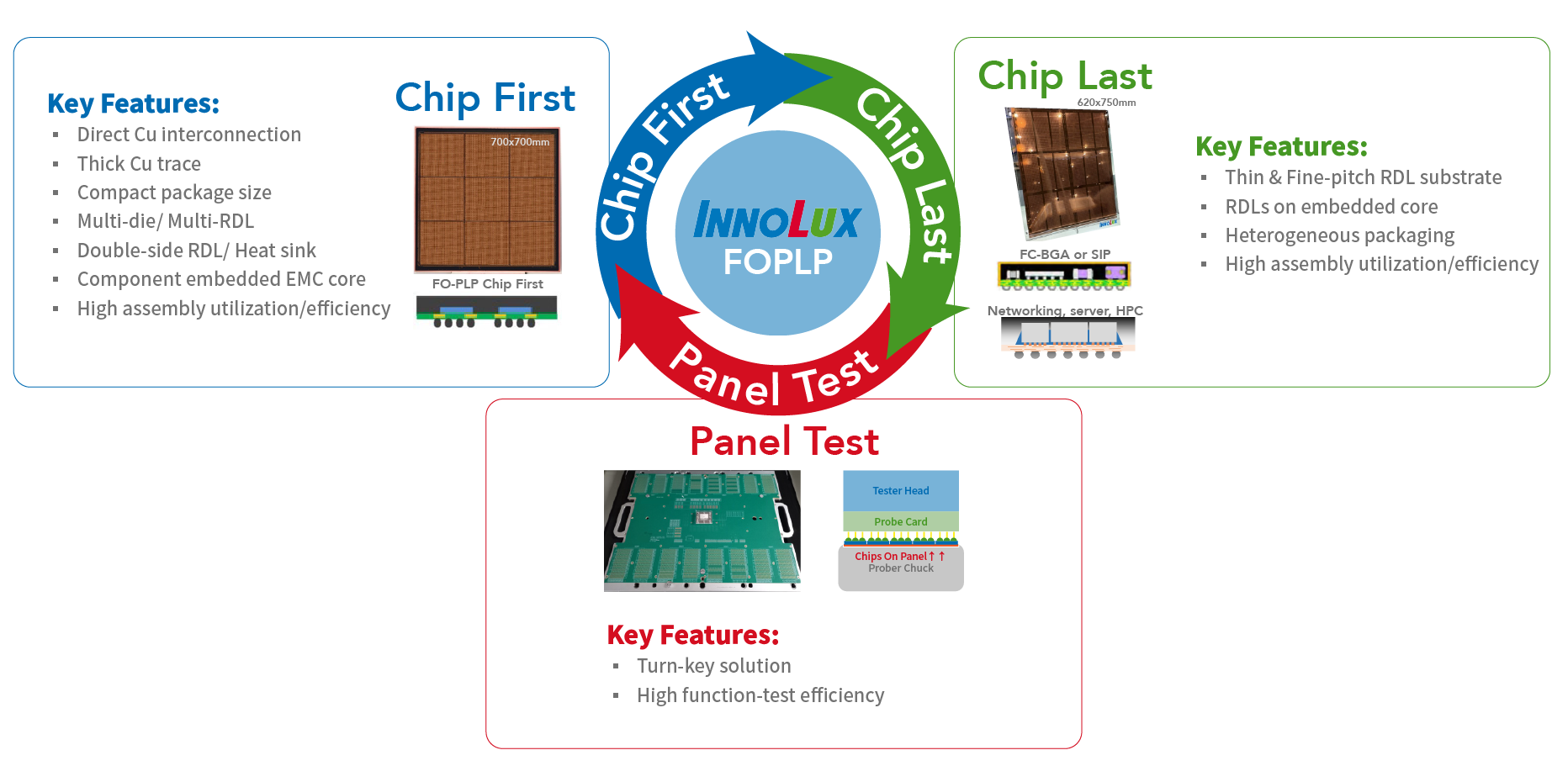
Innolux is setting a new trend in semiconductor packaging with its groundbreaking Fan-Out Panel-Level Packaging (FOPLP) technology. By utilizing the largest FOPLP packaging carriers, this innovative technology fully demonstrates Innolux's ability to transform into a leading semiconductor manufacturer. By setting new standards in performance and efficiency, Innolux is not only shaping the direction of semiconductor manufacturing but also defining the future of FOPLP.
Innolux's FOPLP technology offers a variety of advanced packaging solutions, such as using Chip-First or Chip-Last methods to create packages integrating various components. Innolux's Chip-First technology, in addition to its mass-produced RF satellite antenna applications, is also suitable for manufacturing power devices used in PCs, automotive, and AI or data center servers. Furthermore, Innolux is a supplier of semiconductor substrates for ultra-thin RDL (Redistribution Layer) substrates and Embedded substrates. RDL substrates are key components for manufacturing large AI HPC chip packages, 2.5D packages, and ultra-thin design packages. Innolux also provides panel-level testing services, thereby increasing capacity, minimizing processing time, and reducing total operating costs, ensuring product value and customer satisfaction.
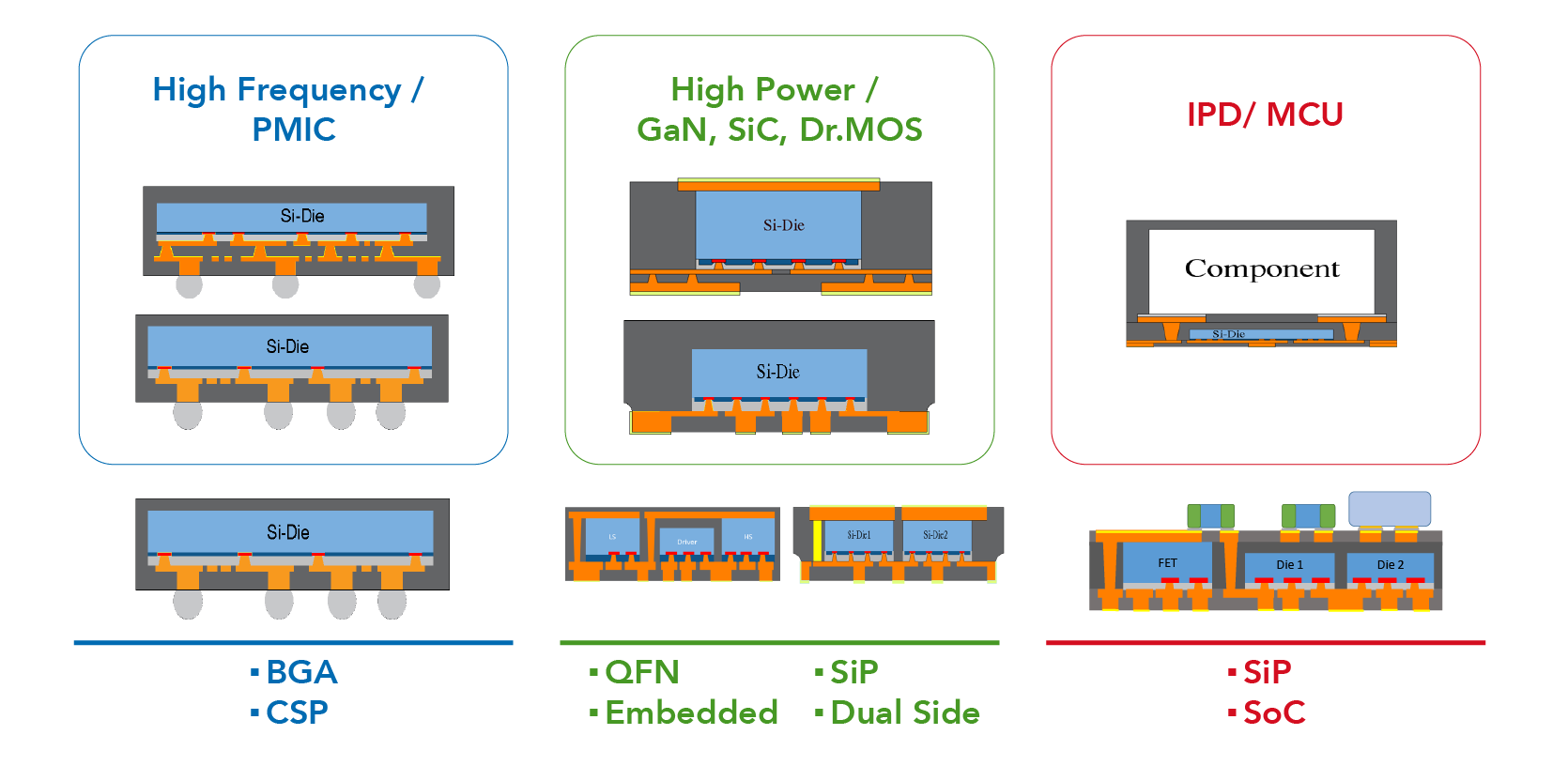
Chip-First Technology Applications
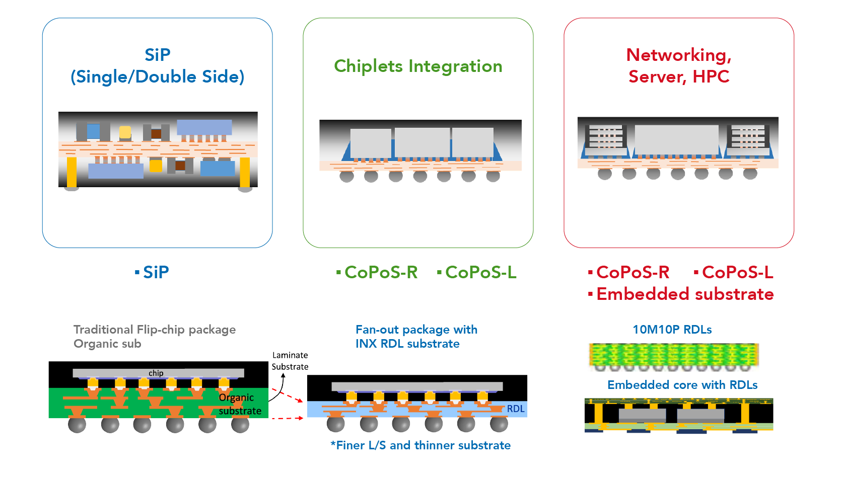
Chip-Last / CoPoS Technology Applications